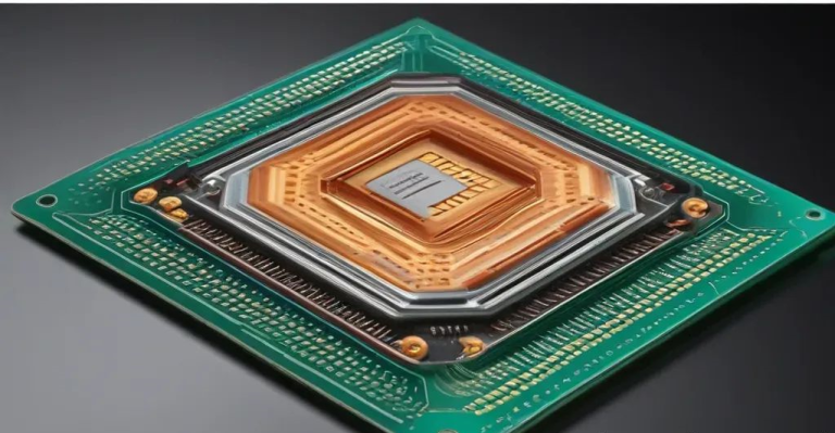
Microchips, which are integral to our digital gadgets, have relied on silicon for decades, making it the bedrock of contemporary computing. But scientists and engineers are looking into new materials and technologies to improve computer chip design and meet the ever-increasing demands for faster and more efficient computing. Discover the fascinating world of non-silicon developing materials and technologies that might change the face of semiconductor technology in this in-depth study.
THE LIMITATIONS OF SILICON:
The physical constraints of speed, power consumption, and compactness are being approached by silicon-based transistors, the cornerstone of contemporary electronics. Quantum processes like electron tunneling and leakage currents become more noticeable when transistor size decrease to nanoscale levels, creating formidable obstacles to additional scaling. New materials and methods with improved performance and scalability are being investigated by researchers as potential solutions to these problems.
EMERGING MATERIALS IN SEMICONDUCTOR TECHNOLOGY:
Gallium Nitride (GaN):
An excellent material for high-frequency and high-power applications, gallium nitride is a wide-bandgap semiconductor with better electrical characteristics than silicon. Improved power conversion and management are made possible in electric cars, renewable energy systems, and 5G wireless networks by GaN-based transistors, which have reduced switching losses, greater breakdown voltages, and better power densities.
Graphene:
The two-dimensional honeycomb lattice of carbon atoms, known as graphene, has tremendous potential for use in next-generation electronics. Graphene may have a huge impact on transistor technology due to its remarkable electrical conductivity, thermal conductivity, and mechanical strength. Transistors made of graphene have the potential to revolutionize computing and communication by allowing for lightning-fast switching rates, reduced power consumption, and greater device integration.
Carbon Nanotubes (CNTs):
Nanostructures made of rolled-up graphene sheets, known as carbon nanotubes, have exceptional mechanical and electrical capabilities. In comparison to silicon transistors, CNT-based transistors have better electron mobility, which results in quicker switching rates and reduced power consumption. The ability to synthesis CNTs on flexible substrates opens up exciting new possibilities for biomedical and wearable electronics, as well as other forms of flexible electronics.
Quantum Dots:
The electrical and optical characteristics of quantum dots, which are semiconductor particles on the nanoscale, vary with their size. The electrical band structure and optical features of these microscopic structures may be precisely controlled because to quantum confinement phenomena. There are a variety of possible uses for light-emitting devices and transistors based on quantum dots, including displays, sensors, and quantum computers, due to their scalability, color purity, and energy efficiency.
TECHNOLOGICAL ADVANCES IN SEMICONDUCTOR MANUFACTURING:
To get around the problems with conventional lithography and patterning procedures, scientists aren’t only looking at novel materials; they’re also improving semiconductor production processes. Nanoimprint lithography (NIL), directed self-assembly (DSA), and extreme ultraviolet (EUV) lithography are some of the techniques that allow for the manufacture of ever more complicated nanostructures with feature sizes less than 10 nanometers. If new materials are to reach their full potential in semiconductor technology, these developments are crucial.
CHALLENGES AND FUTURE PROSPECTS:
While new materials and technologies provide exciting possibilities for semiconductor design innovation, there are a number of obstacles that need to be overcome before they can be widely used. Making sure it works with what’s already out there in the fabrication business, making it more pure and consistent, and increasing production to satisfy demand are all on the list. To fully utilize the possibilities of new materials in practical applications, researchers must also keep exploring innovative device topologies, integration techniques, and dependability mechanisms.